
Oct 17, 2018
Hermetic packaging for semiconductor chips
Physical Sciences, Electrical Engineering
- Efficient protection from the atmosphere
- Thermal resistance reduction
- Induction and parasitics effects reduction
Your contact
Dr. Sindre W. Haugland
- E-Mail:
- shaugland@baypat.de
- Phone:
- +49 (0) 89 5480177 - 17
- Reference Number:
- B76018
Factsheet
Download Tech Offer (PDF)Challenge
The thermal management and the miniaturizaiton are key-aspects in the construction of semiconductor chips. Another important aspect is the minimization of the inductance, which must be kept as low as possible in order to reduce parasitic effects and high voltage peaks. Furthermore, humidity and corrosive atmosphere cause degradation of the semiconductor elements. Standardly, the semiconductor elements are mounted on one side of a direct bonded copper (DBC) and all other electric contacts are provided thorugh wire bonds. This construction is relatively easy to realize, but it provides a bad heat-dissipation and a bad protection from the atmosphere and causes a high inductance. 3D-modules are currently available on the market. Such 3D-moduls solve some of the afore mentioned problems, but their manufacturing process is complex and expensive.
Innovation
The invention consist of a 3D hermetic packaging concept. Semiconductor elements (MOSFETs or IGBTs) soldered on a DBC are hermetically insulated with a cap. Futher the elements can be soldered between two DBCs, creating an ordered 3D-strucuture. This construction can be buildt in few steps, limiting the costs of the manufacture. It additionally provides the following advantages:
- the semiconductor elements are efficiently protected from the atmophere;
- the heat is dissipated in two directions, reducing the thermal resistance up to 56,3%;
- no wire bonds are needed, drastically reducing the inductance and the failure rate due to parasitic effects.
-
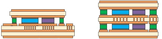
Figure: Two examples for hermetically encapsulated sandwich modules according to invention with optimized materials, geometries in respect to minimization of parasitic induction and optimized thermo-management. The orange and yellow parts represent the DBC and the caps, the blue part respresent an IGBT (or alternatively a MOSFET) and the violett part respresent a diode. The green part respresents the soldering or sintering points. The whole structure is isolated fron the invironment. The two-sided contact ensures the optimization of the thermo-management. Compared to a stardard structure having the same semiconductor elements, the thermal resistance of the left structure 47,7%. Doubling the semiconductor elements as in the right structure leads to a thermal resistance of 87,9% with respect to the same standard structure. Figures adapted from (1).
Commercial Opportunities
The invention can be of advantage for all application for which semiconductor chips are used; in particular for automotive, electromobility and power electronics.
Development Status
The improved heat dissipation has been shown by computer simulations(1).
References
-
- M. Schmidt et. al. „Power Electronic Package for Double Sided Cooling Utilizing Tile-Level Assembly“, PCIM 2017.
- EP 3 223 306 A1, EP 3 240 027 A1.